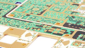
Major function of PCB is to connect the electronic components with the use of conductive path ways and signal traces. It consists of conductive tracks, pads and other features which are etched from copper sheets and laminated onto a conductive substrate. It can be single layered i.e one copper layer or double layered i.e two copper layers or multi layered basing on the requirement. Now coming to a special PCB i.e plating gold PCB where in the process of manufacturing PCB, plating gold is to deposit a layer of gold plated over a barrier coat of nickel by electroplating.

 Successfully Dealing with Difficult People: The 5 Most Difficult Types of People and How to Effectively Approach Them
 Can a Psilocybin Mushroom Trip Really Help Ease Anxiety?
 Visit Myfinal11 Website
 Visit Myfinal11 Website